
Intel Layoffs 2026: Displaced Chip Talent and Where It’s Going
Intel’s 2025–2026 restructuring eliminated more than 25,000 positions under CEO Lip-Bu Tan, dropping headcount from roughly 125,000 to under 100,000. The displaced pool is concentrated in Hillsboro, Chandler, Folsom, and Santa Clara, and it includes RTL designers, physical design engineers, verification leads, and foundry process engineers the rest of the chip industry has been trying to source for years.
Last updated: April 27, 2026
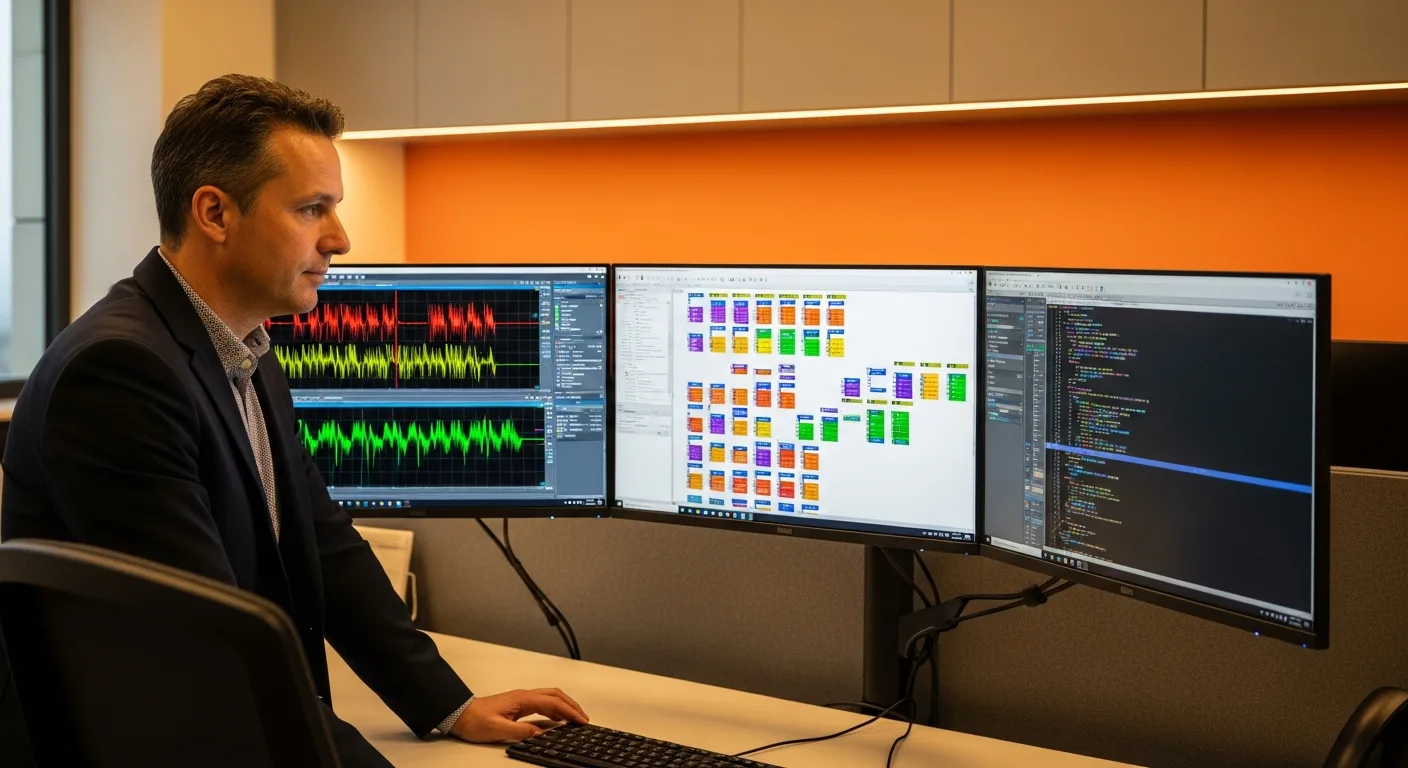
Robert Ardell here. I run engineering search at KORE1’s engineering staffing practice, and a meaningful chunk of every week since November has been spent on the phone with ex-Intel engineers. Not the press-release pool. The actual engineers. RTL, DFT, physical design, packaging, validation, process integration. The profiles that don’t show up in a generic “tech layoff” recap because they don’t fit the SaaS narrative. They’re not the same people. They never were.
One thing to put on the table early. KORE1 collects a placement fee when companies hire engineering talent through us, semiconductor and electrical work included. So when I tell you a usable bench just opened up, I benefit from that being true. Doesn’t change whether it’s true. Read it however you want.
If you’re closer to the WSJ headline than to a fab cleanroom, the headline number gets repeated everywhere. The useful number is who specifically left, where they sit geographically, and how fast they’re being absorbed by TSMC Arizona, the hyperscalers, and the AI silicon startups. That’s the story. Not 25,000 as an abstract.
What Intel Actually Cut, and When
The 25,000 number didn’t come from one announcement. It came from three.
August 2024 was the original 15,000-position reduction Pat Gelsinger announced before the board ousted him in December, framed at the time as a $10 billion cost-savings program tied to the foundry strategy and the AI accelerator roadmap that hadn’t yet shown a credible answer to Nvidia. The cuts started in Q4 2024 and ran through the first half of 2025. Hillsboro took the largest absolute hit. Israel and Ireland got proportional shares. Santa Clara HQ took a manager-layer trim. None of that was the end of it.
March 2025 Lip-Bu Tan came in. He said the quiet part out loud on his first earnings call: too many managers, not enough engineers shipping product, and a foundry business that was burning cash without enough committed external customers to justify the capacity. The follow-on reductions started in Q2 2025 and stretched into early 2026, focused on middle management, the Network and Edge Group, parts of Client Computing, and a meaningful slice of Intel Foundry Services field engineering.
| Period | Approximate Reduction | Where the Cuts Landed |
|---|---|---|
| Q4 2024 – H1 2025 | ~15,000 | Across-the-board, with concentration in Hillsboro, Santa Clara HQ, and the international sites in Leixlip and Kiryat Gat. Manager layer hit hard, plus marketing, sales operations, and select R&D groups. |
| Q2 2025 | ~5,000 | Network and Edge Group consolidation, parts of Client Computing Group, Mobileye-adjacent business units. Folsom and San Diego absorbed disproportionate shares of the Network and Edge cuts. |
| Q3 2025 – Q1 2026 | ~5,000+ ongoing | Middle management trim under Tan’s “flatter org” framing, IFS field engineering after the company shelved 18A external customer ramp targets, additional Hillsboro process integration cuts as 20A was canceled. |
Headcount, on the public record. End of 2023, around 124,800 worldwide. End of fiscal 2025, under 100,000. Reuters has tracked the announcements as they landed; the Crunchbase tech layoffs tracker lists Intel as the single largest contributor among chip companies to the 2024-2026 reduction wave. For broader context across the rest of the year’s tech reset, our tech layoffs 2026 overview walks through Oracle, Amazon, Meta, Microsoft, and the others in the same window.
One nuance worth flagging. WARN filings undercount Intel. A lot of Hillsboro and Santa Clara reductions ran through voluntary separation packages and accelerated retirement offers for senior staff. Those people don’t show up on a state’s WARN list. They show up on LinkedIn three weeks later with “open to work” and a quiet message in your inbox.
The Talent Profiles Most Hiring Managers Are Underestimating
Here’s where the SaaS-layoff playbook breaks down.
An ex-Salesforce admin lands at Deloitte or another partner shop inside six weeks. The pipeline is built. The certifications transfer cleanly. The vendor ecosystem absorbs the supply. Semiconductor talent does not work this way. The certifications don’t exist in the same form. The hiring is concentrated among maybe twenty companies globally that can meaningfully use a senior physical design engineer with 7nm tape-out experience, and several of those twenty are themselves laying off or holding hiring flat at the senior level while they digest acquired teams. The interview loops are six weeks long. The non-competes occasionally get enforced. The geographic concentration matters more than almost any other tech category, because you can’t relocate a fab and you generally can’t relocate the fifteen-year veteran who knows that fab’s quirks either.
The profiles I’m seeing most often, in rough order of pipeline volume:
RTL design engineers (Verilog, SystemVerilog). Mid-level to staff. The bulk of the displaced design pool came from Client Computing Group projects that got shelved or de-scoped. Many had 7nm or 4nm tape-out experience on Meteor Lake, Arrow Lake, or Lunar Lake silicon. That’s marketable to AMD, Apple’s silicon team, Nvidia, Qualcomm, and the AI accelerator startups overnight.
Design verification engineers running UVM with formal experience. Smaller pool than RTL. Higher leverage. A senior DV engineer who can run a full coverage closure on a non-trivial IP block is one of the harder hires in the entire chip industry. The ones leaving Intel right now are landing in 2-4 weeks if they’re not geographically picky.
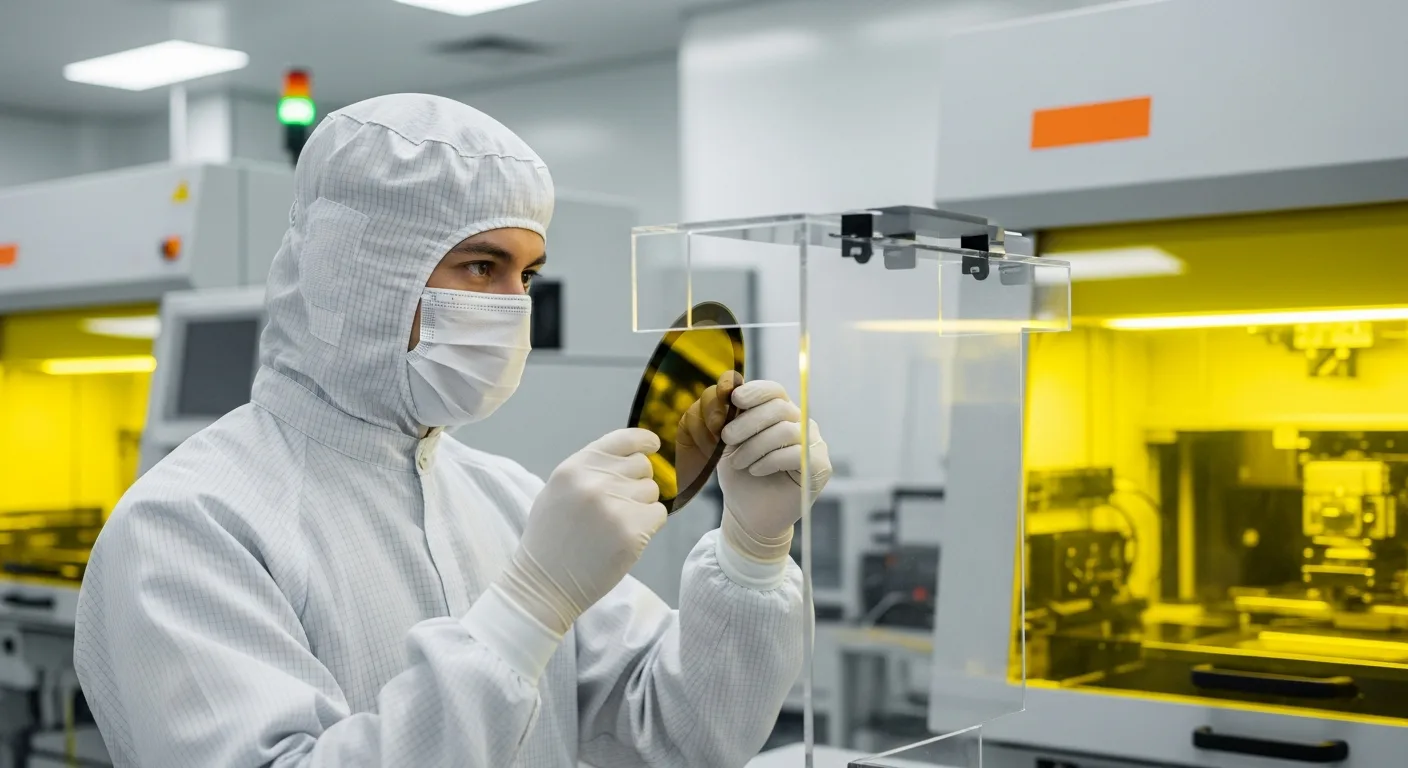
Physical design engineers, particularly those running Cadence Innovus or Synopsys Fusion Compiler on advanced nodes, are a third bucket. Hillsboro had a big one. DFT (Design for Test) and silicon validation engineers are a fourth, and they’re closing fastest because every chip startup needs them and almost nobody has trained any in the past five years. Process integration and yield engineers from the fab side are a fifth, and that pool is moving primarily to TSMC Arizona, GlobalFoundries Malta, and Samsung Austin, not back into the Intel ecosystem.
What I’m not seeing as much of, despite the press coverage: large numbers of senior architects from the central architecture group. Intel mostly held onto those. The cuts there were narrower than the headline implied.

Where Displaced Intel Engineers Are Actually Going
A few destinations dominate. The geography matters as much as the profile, so I’ll group by where people are landing rather than what title they had.
TSMC Arizona, Chandler. Phoenix metro is the single largest absorber of displaced Intel fab and process talent right now. Fab 21 is ramping 4nm and 3nm in 2026 and 2027, and TSMC has been recruiting Intel Ocotillo process integration, lithography, etch, and yield engineers since the layoffs landed. The non-compete question comes up; in Arizona it’s largely moot because Arizona is not a state where Intel’s standard non-competes hold up well. The Semiconductor Industry Association projects domestic semiconductor manufacturing employment will need to grow by 67,000 jobs through 2030 to meet CHIPS Act-funded fab capacity, and TSMC Arizona alone accounts for several thousand of those.
AMD and Nvidia. Every senior Intel RTL or physical design engineer with credible advanced-node experience is getting the call. AMD’s Austin and Santa Clara design centers have absorbed dozens of ex-Intel client and server CPU engineers; Nvidia’s data center GPU and Grace CPU teams are pulling from the same pool. Comp jumps 25–60% on the move, depending on level. The interview loops are brutal. Most candidates close in 6-10 weeks if they make it through.
Apple silicon. Apple has been quieter about its Intel hiring than the press suggests, but it’s significant. The Folsom graphics and media engineering pool is a particular target — Apple’s display and media silicon teams have been pulling from it for two years and the 2025-2026 reductions just made the pool larger. Cupertino-relocate or remote-friendly senior roles primarily.
The AI silicon startups. Cerebras, Groq, SambaNova, Tenstorrent, Rain Neuromorphics, MatX, and a handful of others. These shops hire senior chip designers and verification engineers in volume relative to their headcount. Equity heavy, base modest by Intel standards, but the upside is real for the ones that land. Tenstorrent in particular has been openly recruiting Intel alumni; their CEO is ex-AMD chip design and the cultural fit lands well.
Defense primes and federal integrators. Raytheon, Northrop Grumman, Lockheed Martin, BAE Systems, and L3Harris all hire cleared chip engineers for radar, electronic warfare, and trusted foundry programs. Slower hiring cycles, lower comp than the AI startups, but stability and clearance-leveraged comp bands compete better than they used to. A chunk of the Hillsboro and Folsom population is choosing this path for the second half of a career rather than chasing another roller coaster.
Automotive Tier 1s and Mobileye-adjacent work. Less visible in press coverage but real. Bosch, Continental, Aptiv, Magna, Qualcomm Automotive, and Mobileye itself (which is a separate public company now) hire from the displaced Intel pool, particularly engineers with embedded or vision processing background. Lower volume than the others, but the work absorbs a profile that doesn’t have a clean home elsewhere.
| Profile | Primary Destinations | Time to Close |
|---|---|---|
| RTL / SystemVerilog design engineer | AMD, Nvidia, Apple silicon, Qualcomm, AI silicon startups | 6–10 weeks. Hyperscaler interview loops slow this down. |
| Design verification (UVM, formal) | Same as above + automotive Tier 1s + defense primes | 2–4 weeks. The fastest-closing profile in the entire bench. |
| Physical design (advanced node) | AMD, Nvidia, Marvell, Broadcom, AI startups | 4–8 weeks. |
| DFT / silicon validation | Every shipping silicon company. Especially Apple, Qualcomm, AI startups. | 2–6 weeks. Severe undersupply industry-wide. |
| Process integration / yield | TSMC Arizona, GlobalFoundries, Samsung Austin, Micron | 3–6 weeks. Geographic relocation often required. |
| Firmware / silicon bring-up | Hyperscaler in-house silicon teams (AWS Annapurna, Google Axion), automotive, AI startups | 4–8 weeks. |
Compensation across these moves varies more than most candidates expect. Levels.fyi data puts senior Intel hardware engineers in the $190K–$260K total comp band. AMD and Nvidia offers for the same level are landing in the $260K–$400K range, with the Nvidia number sitting on the higher end if AI-adjacent. Apple sits between. The AI startups quote $180K–$240K base plus equity that’s worth either nothing or a great deal depending on the company. TSMC Arizona is closer to the Intel band. Defense primes 10–20% lower on base with longer-tenure benefits.
What This Means for Your Chip or Hardware Hire in Q2 and Q3
If you’re hiring on the silicon, embedded, or hardware side and you have an open req that’s been sitting more than 60 days, this is the window. Specifically.
The Q2 displaced pool is the highest-quality cohort I’ve seen in this profile in five years. The voluntary separation packages pulled out senior staff who would never normally test the market, often principal engineers a decade past the point where retention bonuses still moved the needle, and the result is a small but meaningful population of people with experience the rest of the chip industry literally cannot recreate from scratch. The 18A foundry pivot opened a door at the IFS level that wasn’t open in 2024. TSMC’s Arizona ramp, while massive, can only absorb so many people before its own loops bottleneck and the in-state Phoenix recruiting market starts pricing every candidate against the same offer letter from Hsinchu. The overflow is real and it’s available.
Across the past 12 months, our average time-to-hire on technology roles has been 17 days from kickoff to first interview. On displaced-Intel engineers specifically, that timeline is running tighter — closer to 10 to 14 days, because the inbound volume from referrals lets us pre-screen faster than a cold sourcing pull. KORE1’s 92% 12-month retention rate has held on these placements through Q1, which matters because chip engineers leaving Intel tend to be evaluating two or three competing offers and the wrong-fit risk is higher than usual.
One last thing on this. I get asked weekly whether the AI silicon startups are actually a viable landing for someone with a mortgage and a teenager headed for college. Honest answer: it depends on the company, the round, and the person. Tenstorrent, Cerebras, and Groq have raised enough that the comp packages are real. Several others have a runway question. If you’re a hiring manager evaluating a candidate who interviewed at one of these and turned it down for your role, that’s a signal worth weighing. It’s not a red flag.
The Geography Question
Most hiring managers underweight this part. Chip work is geographically sticky in a way SaaS isn’t.
Hillsboro and Aloha, Oregon, are the densest concentration of senior process and integration engineers in North America outside of TSMC’s Hsinchu campus, with roughly 22,000 Intel employees working in the region pre-restructuring across D1X, the Ronler Acres campus, and the satellite labs that grew up around the main fab over the past two decades. The displaced pool there is largely staying put. Most of them aren’t relocating to Phoenix or Santa Clara because their spouses have careers and their kids are in good schools and the cost of moving any of that is higher than the comp delta a Phoenix offer would put on the table. They’re waiting for Tualatin and Aloha-area roles to open up at smaller players, at lab equipment vendors like Lam Research and Applied Materials, or at the ramping foundry-adjacent ecosystem. The hiring pace is slower than the cuts. Meaning availability there will outlast the news cycle.
Phoenix and Chandler are the opposite story. TSMC Arizona, Intel Ocotillo, the new Amkor packaging facility, and a growing ecosystem of EDA and equipment vendor field offices have made Phoenix the second center of gravity for U.S. semiconductor work. The displaced Intel pool there is moving fastest. If your hire is Phoenix-based and chip-adjacent, you have weeks, not quarters.
Folsom is graphics and media silicon. Apple, Nvidia, AMD, and a few automotive Tier 1s are the primary absorbers. Folsom moves at a moderate pace — slower than Phoenix, faster than Hillsboro.
Santa Clara HQ is where most of the manager and corporate cuts landed. Less specialized, more abundant elsewhere, but also a population that’s been through this kind of reset before and tends to land quickly.
Common Questions From Hiring Managers
How long is the displaced-Intel availability window actually open?
For the highest-leverage profiles (DFT, senior verification, advanced-node physical design), 60 to 90 days from separation. For everyone else, six to nine months.
The short pool gets called by AMD, Nvidia, Apple, and the funded AI startups within the first month. The longer-tail pool — Hillsboro process engineers waiting on local roles, Santa Clara managers retraining for adjacent fields, Folsom mid-level designers — sits on the market longer and gets selective about the next move.
Will Intel try to enforce non-competes?
Rarely, and not consistently across states.
California won’t enforce them at all. Arizona courts have been inconsistent and tend to side with the employee unless the role is unusually narrow. Oregon enforces only with a clear written agreement signed at hire and limited scope. Practically, Intel has not made a habit of suing departing engineers for working at a competitor, with one or two well-known exceptions involving senior architects. For most candidates and most roles, this is a non-issue.
What kind of comp premium is required to close one of these candidates?
15–30% above their final Intel base for senior engineers. Less for fabs, more for AI silicon work.
The comp expectation depends heavily on what other offers are in front of the candidate. Someone interviewing only with you and a defense prime is more flexible than someone deciding between you and a Series C AI silicon startup with a senior staff offer. We pull comp benchmarks at intake before we present any candidate; the data goes from the recruiter directly to the hiring manager so the negotiation isn’t running blind.
Is a former Intel engineer worth hiring if my company isn’t doing chip design?
Often yes, depending on the profile.
Firmware and silicon validation engineers transition cleanly into embedded systems work, IoT, automotive, and any product company shipping its own hardware. RTL designers with FPGA experience port into specialized industries — defense, aerospace, financial trading hardware. The jump from chip design into pure software is harder and rarer; if that’s the role, screen carefully.
Are the Israel and Ireland reductions producing a usable U.S. pipeline?
Limited. Visa logistics make this slower than you’d expect.
Kiryat Gat and Leixlip alumni are well-credentialed but the H-1B cap and the long timelines for permanent residency conversion make most of these candidates impractical for U.S. hires unless your company already runs a robust visa-sponsorship program. The exception: candidates who already hold green cards or U.S. citizenship from prior tours, of which there are several hundred between the two sites.
How fast can KORE1 actually move on this?
First three submittals inside seven business days for most chip and hardware roles.
Our intake calls run 45 to 60 minutes and we don’t put a single candidate in front of you until we’ve talked to at least three. The bench is current — a meaningful piece of it sits in our pipeline already from prior placements and inbound referrals. Reach out to our team if you want to start the conversation, or look at our semiconductor staffing and electrical engineering staffing pages for what we cover.

One Closing Observation
Intel’s restructuring is unfinished. Tan has signaled more cuts coming if the foundry business doesn’t hit external customer commitments, and the 18A external ramp targets keep slipping. That means the displaced pool isn’t a fixed, closed set. It’s a rolling cohort.
Plan accordingly. The chip engineers leaving in Q2 are not the same profile as the ones who left in Q4 of last year. The Q3 cohort, if there is one, will look different again. If you’re hiring on this profile, the relationship with whoever’s tracking the pool matters more than the static job description on your careers page.
That’s true of most hiring. It’s especially true here.
Common Questions
Is a former Intel engineer worth hiring if my company isn’t doing chip design?
Often yes, depending on the profile. Firmware and silicon validation engineers transition cleanly into embedded systems work, IoT, automotive, and any product company shipping its own hardware. RTL designers with FPGA experience port into specialized industries like defense, aerospace, and financial trading hardware.